Contact Resistance
By defining contact resistances in a simulation, it is possible to account for additional thermal resistance on contacts between volumes. This is especially useful when dealing with very thin layers of solid materials, as it allows users to account for the thermal resistance without having to mesh a thin part.
The contact resistance definition takes place under advanced concepts exclusively for the Conjugate Heat Transfer (IBM) analysis type.
Note that the definition of additional thermal resistances is also available for Conjugate Heat Transfer, however, this is done in the Contacts tab, as described in this documentation page.
Approach
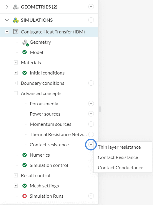
In the simulation tree of a conjugate heat transfer (IBM) simulation, navigate to Advanced Concepts and create a new Contact resistance by clicking on the ‘+’ button. Three options are available: thin layer resistance, contact resistance, and contact conductance.
The three different types of definitions are interchangeable, meaning that you can obtain the same resulting thermal resistance with any of them. Any contact that does not receive a contact resistance will be treated as thermally coupled.
Important
The thermal resistances are applied on each of the assigned faces. As such, this result control will usually be assigned to a single face of a given contact.
Thin Layer Resistance
With a Thin layer resistance contact definition, users can model the additional thermal resistance due to a layer with a certain thickness and thermal conductivity:

Note that only one face of the contact is assigned to the thin layer resistance contact in the image above. If we were to assign both faces of the contact, SimScale would interpret this as two layers of 1e-4 meters of thickness and 10 \(\frac{W}{m.K}\) of thermal conductivity.
Contact Resistance
The Contact resistance interface allows users to model an imperfectly matching interface (e.g. due to the surface roughness) which reduces the heat exchange across it. The total resistance is defined as:
$$ R = \frac{1}{K A} = \frac{1}{\frac{\kappa}{t} A} = \frac{t}{\kappa A} \tag{1} $$
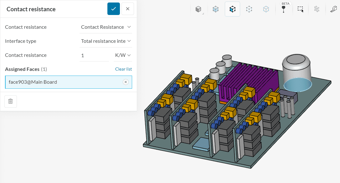
It is worth noticing that the area of the interface appears in the formula, so this option must be assigned only to the relevant face.
A second type of definition is available, now with a Specific resistance for the interface type:
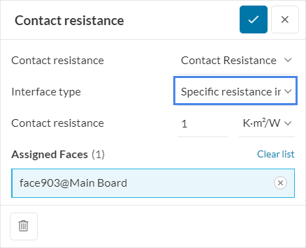
In this case, the value to be defined is the thickness of the layer \(t\) divided by its thermal conductivity \(\kappa\):
$$ R A = \frac{1}{K} = \frac{1}{\frac{\kappa}{t}} = \frac{t}{\kappa} \tag{2} $$
Contact Conductance
When in Specific conductance interface mode, this interface requires users to set the specific conductance of the interface \(K\), which is defined as:
$$ K = \frac{\kappa}{t} \tag{3}$$
with thickness \(t\) in \([m]\) and thermal conductivity \(\kappa\) in \([\frac {W}{mK}]\) between the two interface regions.

For instance, this option may be used for an interface where the layer thickness is negligible or unknown, i.e., a radiator for which the paint coating’s specific conductance may be given instead of its thickness and \(\kappa\).
The last option involves a Total conductance interface definition, where the area \(A\) of the surface is also taken into account in formula 3 above, yielding formula 4:
$$ K = \frac{\kappa A}{t} \tag{4}$$
All in all, the best option for the contact definition depends on what information is available to the user.
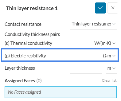
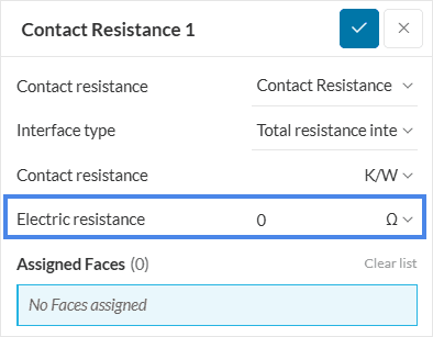
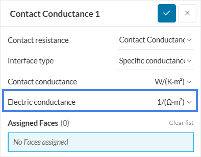
Contact Resistance with Joule Heating
When Joule heating is activated under global settings it is important to take into account the electric properties at the contact surface. The three types of contact resistances described above require an additional electric property to be specified as described below:
Electric Resistivity
- Electric Resistivity (\(\rho\)): This is a material property that quantifies how strongly a material opposes the flow of electric current. It depends on the material itself and is measured in Ohm-meters \([Ω·m]\).
- Electric Resistance (\(R\)): This is the opposition to current flow within a specific object or component, determined by both, the material’s resistivity (\(\rho\)) and the object’s dimension \((l)\). It is measured in Ohms \([Ω]\).
$$R=\frac{\rho}{l} \tag{5}$$
- Electric Conductance (\(G\)): This is the ease with which an electric current flows through an object, essentially the inverse of resistance. It’s measured in Siemens \([S]\), which is equivalent to \([1/Ω]\)
$$G=\frac{1}{R} \tag{6}$$
Last updated: January 22nd, 2026
Did this article solve your issue?
How can we do better?
We appreciate and value your feedback.