Your schematic is clean. Your layout is not.
Every trace, via, and plane introduces unintended resistance, inductance, and capacitance. At low speeds these parasitics are negligible. At high frequencies they cause signal degradation, voltage overshoots, and EMI failures that no amount of debugging will fix after the fact.
PCB parasitic extraction is how you quantify these effects before you fabricate. SimScale runs the full electromagnetic analysis in your browser, turning your 3D layout into an accurate RLC model ready for SPICE or ADS simulation.
Launch your own signal integrity simulation today!
Accurately extract RLC parameters to predict EMI, reduce crosstalk, and ensure first-pass success, all within your web browser.

What Is Signal Integrity and Why Does It Break Down?
Signal integrity (SI) refers to the ability of an electrical signal to travel from a transmitter to a receiver without corruption. In low-speed designs, SI is rarely a concern. At high frequencies (DDR memory, PCIe, RF, and power converter switching nodes) it becomes the dominant design challenge.
Signal integrity problems fall into three categories:
- Reflections: caused by impedance discontinuities along a trace, often from parasitic capacitance at vias or pads
- Crosstalk: electromagnetic coupling between adjacent traces driven by mutual capacitance and inductance
- Power delivery noise: ground bounce and supply rail collapse from parasitic inductance in the power delivery network (PDN)
Parasitic extraction is the process of quantifying these unintended RLC elements from the physical geometry of your PCB before the board is manufactured. The extracted values feed directly into SPICE or ADS simulations, giving you a circuit-accurate model of your layout.

Signal integrity is not a post-layout problem. It is a design space problem. Catching it early through simulation is the only way to avoid costly respins.
Nur Ozturk
Product Manager, SimScale
Signal Integrity and Power Integrity: Two Sides of the Same Problem
Signal integrity (SI) and power integrity (PI) are closely related disciplines that are increasingly analyzed together as SI/PI co-simulation. While SI focuses on data signal quality, PI addresses the stability of the power delivery network that those signals depend on.
Parasitic inductance and resistance in the PDN cause supply voltage to sag or overshoot during switching events, which directly corrupts signal timing margins. A complete parasitic extraction workflow captures both the signal trace parasitics and the PDN parasitics, giving you the full picture.
Understanding Parasitic Elements: The Invisible Design Killers
1. Parasitic Capacitance (C)
The Source: Arises from the electric field between conductive elements (traces, pads, and planes) in close proximity.
The Risk: Causes signal coupling and crosstalk, where a signal on one trace “leaks” into another. It can also create unwanted resonances that shift the impedance of your high-speed lines.
SimScale Solution: Use Electrostatic analysis to extract the full capacitance matrix, identifying stray coupling before you hit the lab.

2. Parasitic Inductance (L)
The Source: Created by the magnetic field generated by current flowing through traces and vias.
The Risk: Inductance opposes changes in current. In power electronics, this leads to voltage overshoots that can exceed the breakdown voltage of your components.
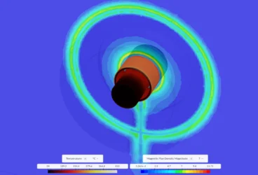
SimScale Solution: Extract loop and self-inductance via Magnetostatic or AC Magnetic solvers to optimize your switching loops.
3. Parasitic Resistance (R) and the Skin Effect
The Source: The inherent property of copper traces and vias to restrict current flow.
The Risk: Beyond simple DC voltage drops, high-speed designs suffer from the Skin Effect, where current crowds to the conductor surface at high frequencies, drastically increasing effective resistance and thermal load.
SimScale Solution: Compute frequency-dependent AC resistance to ensure your Power Delivery Network (PDN) remains cool and efficient.
4. Mutual Inductance and Coupling
The Source: Occurs when the magnetic fields of adjacent conductive paths overlap.
The Risk: Induces noise in sensitive analog circuits or feedback loops, often leading to EMI/EMC compliance failures.
SimScale Solution: Visualize magnetic flux density in 3D to identify where traces are too close and quantify the mutual coupling coefficient.
5. Dielectric Loss
The Source: High-frequency energy dissipation within the PCB substrate and conductor traces.
The Risk: Energy lost to the dielectric material and skin effect manifests as heat. In high-power designs, these hotspots can degrade the substrate and cause thermal expansion that leads to mechanical failure.
SimScale Solution: Couple EM power loss results with thermal simulation to visualize heat distribution, validate cooling strategies, and ensure material reliability.

Key Capabilities
Parasitic Capacitance: Electrostatic Analysis
Use the Electrostatic module to calculate the coupling between signal traces, ground planes, and floating conductors. The output is a full multi-conductor capacitance matrix. Identify stray capacitance that causes unwanted feedback or instability in high-impedance nodes.
| Name | Floating potential 2 (F) | Floating potential 3 (F) |
|---|---|---|
| Floating potential 2 | 4.614268E-12 | −4.151798E-13 |
| Floating potential 3 | −1.651798E-13 | 4.614258E-12 |
DC and AC Resistance: Magnetostatic and Eddy Current Analysis
Extract DC resistance for power integrity and AC resistance to account for Skin Effect and Proximity Effect. Ensure your power delivery network can handle high-frequency ripple without excessive heating.
| Name | Trace 1 (Ohm) | Trace 2 (Ohm) |
|---|---|---|
| Trace 1 | 0.00351044 | 3.56724E-4 |
| Trace 2 | 3.56724E-4 | 0.00953349 |
Parasitic Inductance: L-Matrix Extraction
Quantify inductance in switching loops. Reducing parasitic inductance is critical for minimizing V_DS ringing in power converters and preventing timing violations in high-speed digital lines.
| Name | Trace 1 (H) | Trace 2 (H) |
|---|---|---|
| Trace 1 | 2.19126E-8 | 1.00335E-9 |
| Trace 2 | 1.00335E-9 | 2.19226E-8 |
The Smarter, Faster Way to PCB Parasitic Extraction
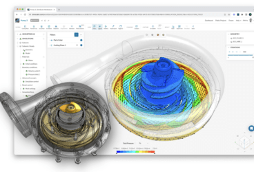
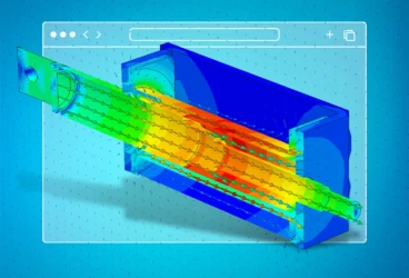
3D Electromagnetic Field Analysis: Move beyond 2D approximations. Visualize 3D current density, detect skin effect bottlenecks, and quantify magnetic flux coupling to eliminate crosstalk in dense layouts.
Thermal-Coupled Electromagnetics Solver: Predict AC/DC copper losses and dielectric heating. Identify hotspots in your Power Delivery Network and optimize your design before hardware prototyping.
Stackup and Geometry Optimization: Rapidly test different dielectric materials, trace widths, and ground plane configurations to balance impedance control, signal integrity, and manufacturing costs.
Noise Immunity Analysis: Evaluate electric and magnetic field distributions to identify traces prone to radiating noise. Minimize unintended coupling early in the design cycle to ensure your board meets stringent signal quality and pre-compliance requirements.
Physics AI Acceleration: SimScale’s AI-native cloud platform uses Physics AI to predict how layout changes impact parasitic values in seconds, enabling rapid design space exploration without waiting for full solver runs.
Application Focus and Use Cases
Power Electronics / Power Converters: Optimize half-bridge layouts to minimize commutation loop inductance and prevent device failure from overvoltage spikes.
High-Speed Digital (HSD): Extract RLC models for DDR, PCIe, and RF traces to perform accurate SI/PI co-simulation.
EMI/EMC Pre-Compliance: Predict radiated and conducted emissions by modeling the PCB as a complex network of parasitic radiators.
Technical Workflow
- CAD Import: Upload your 3D CAD file directly. No file conversion required.
- Material Assignment: Define dielectric constants (e.g., FR4 εr = 4.4) and copper conductivity.
- Solver Setup: Choose between Electrostatic (C), Magnetostatic (DC R/L), or AC Magnetic (AC R/L) analysis based on your extraction target.
- Post-Processing: Visualize 3D field distributions and export the RLC matrix for SPICE or ADS integration.
Everything runs in your browser. No HPC setup, no VPN, no local install required.
Frequently Asked Questions
Signal integrity simulation is the process of using electromagnetic and circuit solvers to predict how signals behave on a PCB before the board is manufactured. It covers transmission line effects, reflections, crosstalk, and power delivery noise. In practice, SI simulation starts with parasitic extraction — quantifying the unintended R, L, and C values from your layout geometry — and feeds those values into a circuit simulator such as SPICE or ADS to predict waveform quality, timing margins, and EMI risk.
Parasitic extraction is the process of identifying and quantifying unintended electrical elements (resistance, inductance, and capacitance) that arise from the physical geometry of a PCB layout. These parasitics are not explicitly designed in but have a significant effect on circuit behavior, particularly at high frequencies. The extracted RLC values are used to build accurate simulation models for signal integrity and power integrity analysis.
Parasitic capacitance forms wherever two conductive surfaces are separated by a dielectric material. Trace-to-trace, trace-to-plane, and pad-to-pad are the most common sources. The closer the conductors and the larger their overlapping area, the higher the capacitance. At high switching speeds, even small parasitic capacitances cause measurable signal degradation.
In switching power converters, parasitic loop inductance in the commutation path causes voltage spikes (V = L x dI/dt) during transistor turn-off. These spikes can exceed the breakdown voltage rating of the switching device, causing failure. Minimizing loop inductance through careful layout and parasitic extraction simulation is a standard practice in power electronics design.
Yes. SimScale’s electromagnetic solvers output capacitance matrices (C-matrix) and inductance matrices (L-matrix) that can be exported as SPICE-compatible netlists or S-parameter files for use in downstream circuit simulators such as LTspice, ADS, or Cadence Spectre.
Signal integrity (SI) focuses on the quality of data signals as they travel between devices, ensuring clean waveforms, correct timing, and minimal noise. Power integrity (PI) focuses on maintaining a stable supply voltage at the point of load, accounting for PDN parasitics such as trace inductance and decoupling capacitor impedance. Modern high-speed designs require SI/PI co-simulation because PDN noise directly affects signal timing margins.