In most electronic cooling applications, there is often the need to define a thermal pad/paste between electrical components, otherwise known as Thermal Interface Materials (TIM).
The main purpose of a TIM is to replace the poorly heat conductive air gap, with a material of higher conductivity between two components, usually a chip and a heatsink. For example, if you take a heat sink and place it on top of a chip, there will still be a very small air gap between the components even though they may seem in contact.
One known aspect of air is that it is a very bad conductor of heat, so that tiny air gap between the heat sink and the chip would act as an insulator and hence reduce the efficiency of heat transfer.
Essentially, the TIM material would then eliminate the air gap and act as a thermal bridge between the chip surface and the heat sink.
Now talking in CFD terms, TIM materials are usually quite thin - few magnitudes smaller than the other components. This means resolving the geometry of a TIM may result in a singificantly large mesh that could be avoided by simply modeling the behavior of the TIM as a contact surface.
Let’s take this example of an electronics box enclosure and see how we can define a thermal interface material as a contact surface between the heat sink and the CPU.
The GIF below illustrates this process:
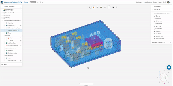
- Choose the parts that you want to define a thermal resistance layer in between them
- Filter contacts by selection → this directly navigates you to the context menu that allows you define the contact defintion between these two parts
- Choose the thin layer resistance interface
- Define the thermal conductivity and thickness of the material
Lastly, if you would like to know how to convert the thermal impedance of your TIM material to an input for the thin resitance layer in CHTv2, then kindly refer to this forum post
If you have any questions please don’t hesitate to contact us.