Hey @irving,
so usually if there is just one value given (e.g. junction to board resistance), it means that the rest of the resistance values can be almost neglected. Otherwise sometimes there are multiple resistances provided by suppliers e.g. additionally junction to case (top) resistance or even to the sides. In most cases at least the side resistances are neglected though.
In theory of course the networks can be as complex as defined by JEDEC:
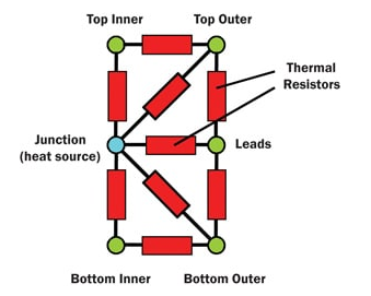
e.g. for reference: Compact thermal modeling in electronics design | Electronics Cooling
To my knowledge the whole point of those compact thermal models though is that they actually represent the actual physics in many cases much better than trying to resolve these parts geometrically in detail. I am dealing mostly with simple chips e.g. LED COB or single chips where those models are very valid. /so I am not sure it is the best approach in your case, but as you don’t have the geometrical details anyways, I think it’s worth a try.
They should now be available to you as the release just happened yesterday by coincidence ![]()
Best Regards
Alex