I am curently working on a Conjugate Heat Transfer simulation and so far I have some trouble generating the mash,
The design consist of one heat producing element (smd transistor) on a double sided PCB. The whole assamble is surounded by air. When I try to generate the mesh as HEX dominant parametric + multiregion mesh, the process terminates with error.
Any advice is more than welcomed!
thank you very much for yor reply!
The thing is, even without the fluid/just the PCB board + Transistor, I get the same mesh error.
It must be something wrong with my CAD Model though I couldn’t find anything.
Would be great if you can have a look at the CAD as there is not much of information in the mesh report, updated link below.
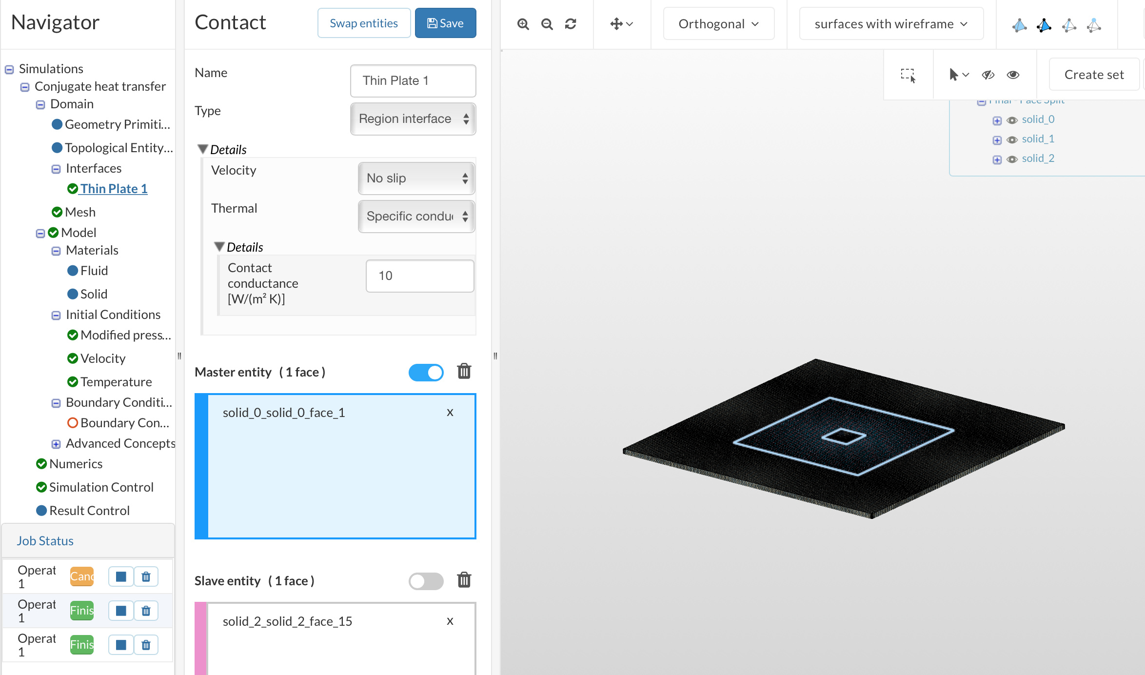
Ok so it seems that it takes a lot of effort to sufficiently mesh the thin plates (there are 3 solids I consider to be ‘thin’) The beta hex-dominant is very good at sorting this as it refines based on geometrical sizing. However, the produced mesh is enormous.
It might then be a good opportunity to try out the TIM feature that allows a thermal resistance interface between faces. I think the best way to start this process is to create geometry that excludes the thin faces but instead has face splits around the parameter on the biggest geometry. If you are using OnShape feel free to share the project with me and maybe I could quickly collaborate and show you visually what I mean. Hopefully, this might be a less expensive solution?
This uses a mere 1 million cells, the alternative involves a mesh that is 32 million + (the point the machine ran out of memory).
Let me know what you think,
Darren
Forgot to say, the assumption of this approach is that conduction is through the plate and none across it. This will not affect results too much but its worth noteing.
With your method is possible to generate the mesh, however this is not what I want.
My goal is to simulate the heat flow from the transistor trough the PCB. The PCB is typically a sheet of FR4 1.6mm thick (low heat conductive) and 2 layers of copper 75um thick (highly heat conductive).
The copper is not only an interface but a heatsink as well. There will be conductive heat transfer from the point where the heating element is located towards the edges of the copper layer, from the copper layer to the FR4 as well as convective heat transfer from the copper to the surounding fluid area (air).
Let me know if you have other ideas.
Hi @dpruna88, I think it would be beneficial if you could upload an image of your geometry annotated with heat sources and what each solid represents. Couldn’t I see any copper layers within your PCB? or are they the thin plates either side? The more information you can give the faster we can move forward. When we talk about meshing something that is 75 um the resulting mesh might be expensive but if conduction across the plate is considered significant it might be necessary.
the objects in the simulation are as follows:
Solid4- SMD transistor (generates heat)
Solid3 - tinn solder joint 100um (conducts heat)
Solid2 and 1 - copper layer 75um thick (conducts heat)
Solid0- FR4 layer 1.6mm thick (conducts heat)
All this values are very standard for electronic industry. Just an example, for 5W of power dissipated by the transistor, temperature gradient on the first copper layer can be as high as 10K. That’s why is so important to simulate the real behavior of the PCB board.